Institute of Materials Science

Research


Scientific Achievements and Impact

Scientists of the Institute are researching micro relief, plasmonic structures, microstructures for solid oxide micro fuel cells, hydrophobic surfaces, diamond-like carbon and diamond like nanocomposite coatings, are developing new periodic and holographic relief structure replication methods and nanocomposite formation. Research results were applied for micro and nanodevices and structures, many of which in the area of document anti-counterfeiting solutions. All of these areas are of upmost importance for Lithuanian and EU industry.

Research carried out by the staff of the Institute is aimed towards micro and nanostructures, microsystems, nanooptics, microelectromechanical, optoelectronic, semiconductor device and related technology development. Research conducted is multidisciplinary and of utmost importance for the society development. Scientific results are disseminated in international conferences, published in top impact factor journals indexed in Clarivate Analytics, Web of Science. The Institute’s staff are also members of editorial boards and referees in various scientific journals.

Most Important Publications

Viktoras Grigaliūnas, Šarūnas Meškinis, Dalius Jucius, Algirdas Lazauskas, Mindaugas Andrulevičius, Asta Guobienė, Brigita Abakevičienė, Mindaugas Juodėnas, Rimantas Gudaitis, Vitoldas Kopustinskas, Andrius Vasiliauskas, Albinas Kasparaitis. Anti-fogging technique for protection of optical grating scales (2023). Optical Materials.

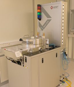
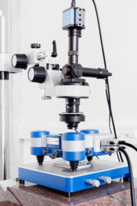
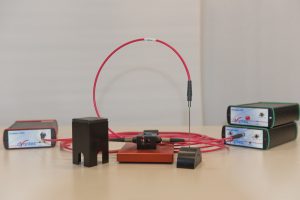
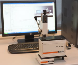
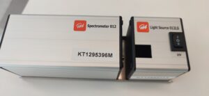
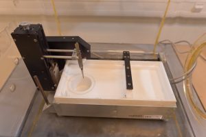
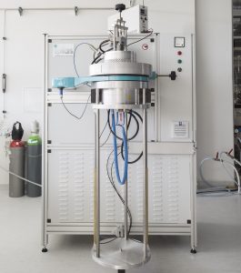
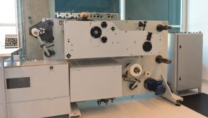
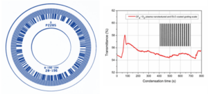
The combined technique consisting of CF4/O2 plasma nanotexturing of the glass surface and the deposition of the SiOx containing DLC film on the top of the grating scale followed by O2 plasma treatment was designed for the long-lasting protection of the optical grating scales from fogging. XPS analysis of the DLC film before and after O2 plasma treatment shows that even short exposure to O2 plasma produces oxidized silicon on the surface of the DLC film. O2 plasma treatment time of 180 s leads to the increase of the carbon C=C peak (sp2 hybridization) intensity from 15% to 32%, and a decrease of the carbon C-C peak (sp3 hybridization) intensity from 67% to 45%. The wetting angle of the plasma nanotextured and DLC-coated optical grating scale retains superhydrophilic properties and optical transmittance after long-term storage. The proposed technique ensures long-lasting operation of the encoder with the optical grating scale below dew point temperature.


Nadzeya Khinevich, Domantas Peckus, Asta Tamulevičienė, Gerda Klimaitė, Joel Henzie, Tomas Tamulevičius, Sigitas Tamulevičius. Size and crystallinity effect on the ultrafast optical response of chemically synthesized silver nanoparticles (2023). Journal of Materiomics

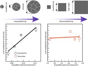
TThis article shows how a transient absorption spectrometer (TAS) can be useful for determining the crystallinity of silver nanoparticles. Silver nanoparticles are interesting because of their plasmonic properties. Localized surface plasmon resonance is known to relax by several processes, such as electron-electron scattering, electron-phonon (e-ph) coupling, and phonon-phonon scattering. Of these processes, the e-ph coupling is the most interesting, as it allows determining where nanoparticles are best used, for example, for photocatalysis (long e-ph coupling) or thermal effects (short e-ph couplin. To determine how the crystalline structure affects the e-ph coupling durations, two types of samples were studied: monocrystalline silver nanocubes and polycrystalline (increasing polycrystallinity with increasing size) silver nanospheres, the sizes of which were in the length range of 30-60 nm. It was found that in monocrystalline nanocubes, the duration of e-ph coupling did not depend on the size of the edge of the cube, while in polycrystalline spheres, the duration of e-ph coupling decreased linearly with increasing diameter. Finally, we have demonstrated that the e-ph coupling decay time constant depends linearly on (Crystallite size / linear dimension of Ag NPs)2 for polycrystalline Ag nanospheres, while monocrystalline Ag nanocubes do not show any clear dependence on this ratio. This fact illustrates that the e-ph coupling time could be used to evaluate crystallinity and crystallite size in plasmonic metal nanoparticles when the size (surface area) of the nanoparticle is known.


Domantas Peckus, Asta Tamulevičienė, Karine Mougin, Arnaud Spangenberg, Loic Vidal, Quentin Bauerlin, Marc Keller, Joel Henzie, Linas Puodžiukynas, Tomas Tamulevičius, Sigitas Tamulevičius. Shape influence on the ultrafast plasmonic properties of gold nanoparticles (2022). Optics Express.

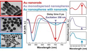
The article shows how ultrafast differential absorption spectroscopy (TAS) can be used to study the sizes, shapes, and homogeneity of plasmonic gold nanoparticles. Scanning electron microscopy or transmission electron microscopy can usually be used quite reliably for these studies, but these measurements are relatively slow, the equipment used is expensive, and the studies involve relatively small amounts of nanoparticles. Typically, measurements of ultraviolet–visible light (UV–VIS) steady-state absorption spectra are used for rapid studies of plasmonic metal nanoparticles. The analysis is simple and fast, and measurement equipment is widely available, so this type of study is very common, but it is difficult for this method to reliably distinguish different forms of nanoparticles. During our research, we found that the dynamic TAS method can help determine the size, shape, or another form of nanoparticle impurities much more reliably and accurately than measurements of steady-state UV-VIS absorption spectra. These results can be useful for studying the properties of plasmonic metal nanoparticles and are of great significance for materials science. This article has been awarded the Editor’s Choice recognition, which is only given to the articles that are significant in their field and have excellent scientific quality.


Agnė Šulčiūtė, Keita Nishimura, Evgeniia Gilshtein, Federico Cesano, Guido Viscardi, Albert G. Nasibulin, Yutaka Ohno, Simas Račkauskas. ZnO Nanostructures Application in Electrochemistry: Influence of Morphology (2021). The Journal of Physical Chemistry C.

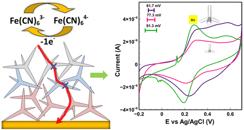
In this work we analyze how a form of zinc oxide (ZnO) nanomaterials determines their electrochemical properties. Different forms of ZnO were compared: tetrapods, nanoparticles and nanowires. ZnO tetrapods synthesized in our laboratory were found to have better electrochemical properties than commercial ZnO (nanoparticles, nanowires). ZnO tetrapods have the highest active surface area (A = A= 0.095 cm2), and the lowest number of electronic transport skaičiaus (DEp = 61.7 mV), which is very close to the theoretical value. This detailed study of the influence of ZnO nanostructure and form on electrochemical properties, will be useful in the development of future biosensors.


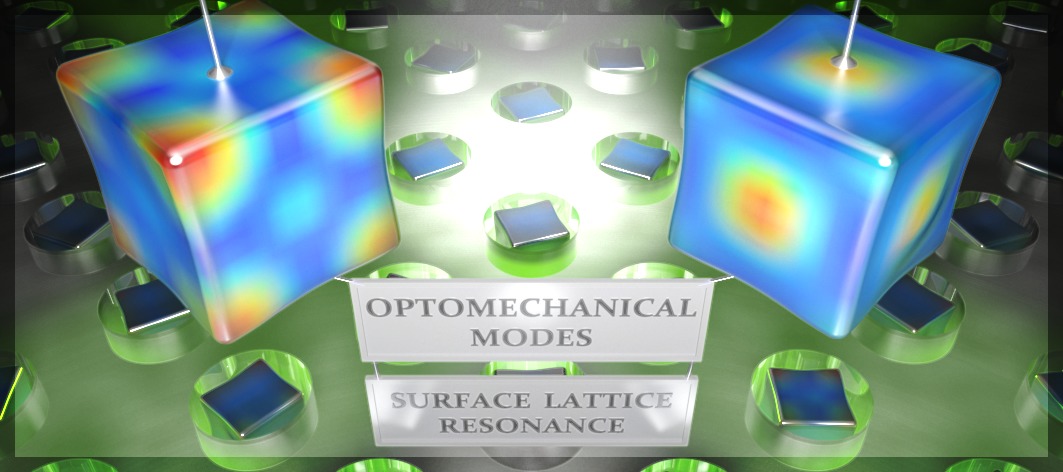
Mindaugas Juodėnas, Domantas Peckus, Tomas Tamulevičius, Yusuke Yamauchi, Sigitas Tamulevičius, and Joel Henzie, Effect of Ag Nanocube Optomechanical Modes on Plasmonic Surface Lattice Resonances (2020). ACS Photonics

This article describes the interaction of ultrafast light pulses with silver nanoparticles and their arrays. We showed that light pulses elapsing a trillionth of a second (1/1 000 000 000 000 s) can excite mechanical vibrations in nanoparticles that are a thousand times smaller than the width of a human hair. These processes can be visualized in dynamic light absorption spectra because the color of plasmonic materials depends on their size and shape which can be modulated by mechanical vibrations. We investigated arrays of such nanoparticles and described the influence of local ultrafast oscillations on a long-range phenomenon—the surface lattice resonance (a collective optical response of regular nanoparticle arrays), which is extremely sensitive to the color of light scattered by the nanoparticles. Our observations will allow to create ultrafast elements of nanophotonics and opens the doors for a new generation of nanolasers.


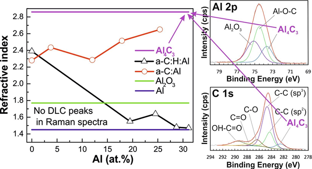
Domantas Peckus, Šarūnas Meškinis, Andrius Vasiliauskas, Erika Rajackaitė, Mindaugas Andrulevičius, Vitoldas Kopustinskas, Sigitas Tamulevičius, Structure and optical properties of diamond like carbon films containing aluminium and alumina (2020) Applied Surface Science

This paper describes the results of studies of diamond-like carbon coatings (coatings containing carbon atoms of different spatial configurations – typical for crystalline diamond and graphite) with different concentrations of aluminum nanoparticles (DLC:Al). We investigated two different types of magnetron sputtering deposited DLC coatings: hydrogenated (coatings also contain hydrogen atoms) and non-hydrogenated with different Al atomic concentrations in them. If the studies of the composition of hydrogenated DLC:Al did not show unexpected results – alumina (AlOx) derivatives were formed in these coatings, then in addition to AlOx compounds, aluminum carbide (AlCx) derivatives were formed in non-hydrogenated DLC:Al. It is known that the formation of AlCx is usually very inefficient and requires temperatures above 1000 oC, therefore most often during synthesis, which takes place at much lower temperatures (e.g. room temperature), no AlCx is formed in DLC:Al films. The fact that we were able to obtain AlCx at relatively very low room temperatures is an interesting result, and the better understanding of the synthesis method we used may contribute to the efficient preparation of AlCx coatings in the future. Thanks to their high thermal conductivity, low thermal expansion and high refractive index, these coatings can be widely applied in optoelectronics. The sufficiently simple magnetron-based coating preparation method described in the article may contribute to the wide practical applications of AlCx in the future.


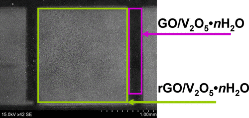
Algirdas Lazauskas, Liutauras Marcinauskas, Mindaugas Andrulevičius, Modification of Graphene Oxide/V2O5• n H2O Nanocomposite Films via Direct Laser Irradiation (2020). ACS Applied Materials & Interfaces

Herein, photothermal modification of nanocomposite films consisting of hydrated vanadium pentoxide (V2O5·nH2O) nanoribbons wrapped with graphene oxide (GO) flakes was performed via 405 nm direct laser irradiation. The combination of X-ray diffraction, X-ray photoelectron spectroscopy, Raman scattering, transmission electron microscopy, and scanning electron microscopy allowed comprehensive characterization of physical and chemical changes of GO/V2O5·nH2O nanocomposite films upon photothermal modification. The modified nanocomposite films exhibited porous surface morphology (17.27 m2 g–1) consisting of randomly distributed pillarlike protrusions. The photothermal modification process of GO/V2O5·nH2O enhanced the electrical conductivity of nanocomposite from 1.6 to 6.8 S/m. It was also determined that the direct laser irradiation of GO/V2O5·nH2O resulted in considerable decrease of C–O bounds as well as O–H functional groups with an increase of the laser power density.


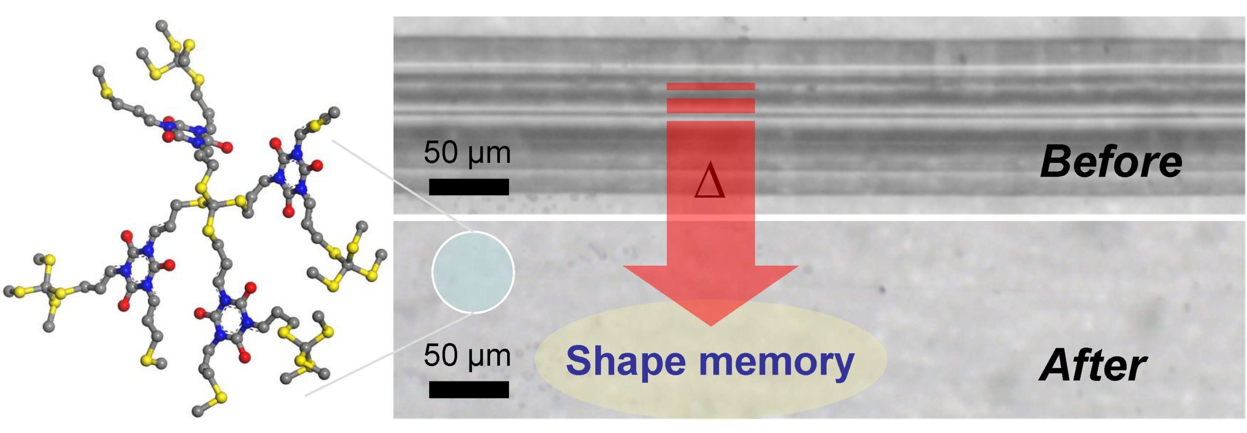
Algirdas Lazauskas, Dalius Jucius, Valentinas Baltrušaitis, Rimantas Gudaitis, Igoris Prosyčevas, Brigita Abakevičienė, Asta Guobienė, Mindaugas Andrulevičius, Viktoras Grigaliūnas, Shape-Memory Asisted Scratch-Healing of Transparent Thiol-Ene Coatings (2019). Materials

This paper reports on the properties of scratch-healing thiol-ene coatings synthesized at the Institute of Materials Science at Kaunas University of Technology on the basis of photopolymerizable composition prepared as a mixture of pentaerythritol tetrakis(3-mercaptopropionate) (PETMP) and 1,3,5-triallyl-1,3,5-triazine-2,4,6(1H,3H,5H)-trione (TTT), with 1 wt. % of 2,2-dimethoxy-2-phenylacetophenone (DMPA) photoinitiator. It was demonstrated that such coatings exhibit high optical transparency, elasticity and shape-memory. The crosslinked PETMP-TTT polymer network was capable to initiate scratch recovery not only under the influence of an external stimulus but also at the room conditions. It was suggested that such coatings could be integrated in a new generation of the optoelectronic products.


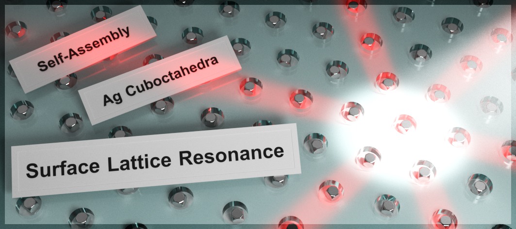
Mindaugas Juodėnas, Tomas Tamulevičius, Joel Henzie, Donats Erts, and Sigitas Tamulevičius, Surface Lattice Resonances in Self-Assembled Arrays of Monodisperse Ag Cuboctahedra (2019). ACS Nano

This article describes a new optical phenomenon—a surface lattice resonance (a collective optical response of regular nanoparticle arrays) and a method to produce the required plasmonic nanostructures using capillary force-assisted nanoparticle assembly. We showed that this extremely wavelength-sensitive phenomenon can be generated by arranging noble metal (gold, silver) nanoparticles on specifically patterned templates. Our method avoids serial writing of individual nanoparticles by using self-assembly to arrange them en masse from a colloidal solution. These surface lattice resonance-featuring nanostructures allow to manipulate light and enhance the electric field both locally and throughout the plane of the array, which is essential for extra-sensitive biosensors and nanolasers.


The scientific potential of scientists and researchers of KTU Institute of Materials Science has gained global reputation by participating in national and international fundamental research and R&D projects.

Patents and patent applications

2021

Patent applications have been registered at the EPO, USPTO, JPO patent offices
1. Fabrication method of holographic security label : Japan patent application / inventors: V. Grigaliunas, S. Tamulevicius, M. Andrulevicius, T. Tamulevicius, E. Fataraite-Urboniene, P. Narmontas, T. Klinavicius, D. Jucius, M. Juodenas; applicant: Kaunas University of Technology. JP 2021170104 A. 2021-10-28.
2. Fabrication method of holographic security label : European patent application / inventors: V. Grigaliunas, S. Tamulevicius, M. Andrulevicius, T. Tamulevicius, E. Fataraite-Urboniene, P. Narmontas, T. Klinavicius, D. Jucius, M. Juodenas; applicant: Kaunas University of Technology. EP 3896529 A1. 2021-10-20.
3. Fabrication method of holographic security label : United States patent application / inventors: V. Grigaliunas, S. Tamulevicius, M. Andrulevicius, T. Tamulevicius, E. Fataraite-Urboniene, P. Narmontas, T. Klinavicius, D. Jucius, M. Juodenas; applicant: Kaunas University of Technology. US 2021318621 A1. 2021-10-14.

2022

Patents registered at the EPO, USPTO, JPO patent offices
1. Fabrication method of holographic security label / inventors: V. Grigaliunas, S. Tamulevicius, M. Andrulevicius, T. Tamulevicius, E. Fataraite-Urboniene, P. Narmontas, T. Klinavicius, D. Jucius, M. Juodenas; applicant: Kaunas university of technology. JP 7000647 B2. 2022-01-19.


Patent applications have been registered at the EPO, USPTO, JPO patent offices

1. An optical device with ordered scatterer arrays for secure identity and a method of producing the same : Japan patent application / inventors: T. Tamulevicius, M. Juodenas, A. Tamuleviciene, T. Klinavicius, S. Tamulevicius; applicant: Kaunas university of technology. JP 2022158738 A. 2022-10-17.
2. Optical device with ordered scatterer arrays for secure identity and a method of producing the same : United States patent application publication / inventors: T. Tamulevicius, M. Juodenas, A. Tamuleviciene, T. Klinavicius, S. Tamulevicius; assignee: Kaunas university of technology. US 2022314682 A1. 2022-10-06. [Espacenet] [M.kr.: T 008] [Indėlis: 1,000]
3. An optical device with ordered scatterer arrays for secure identity and a method of producing the same : European patent application / inventors: T. Tamulevicius, M. Juodenas, A. Tamuleviciene, T. Klinavicius, S. Tamulevicius; applicant: Kaunas university of technology. EP 4067102 A1. 2022-10-05.
2023

“High diffraction efficiency periodic microstructures for optical wavelength range from modelling to implementation”, Andrius Žutautas (technological sciences), scientific supervisor Prof. Dr. Tomas Tamulevičius

2022

“Microwave Plasma-Enhanced Chemical Vapour Deposition and Quality Studies of Planar and Vertical Graphene Layers”, Erika Rajackaitė (technological sciences), scientific supervisor Prof. Dr. Sigitas Tamulevičius

“Nanostructured Metal Oxides Doped Ceria Ceramics for Low-Temperature Solid Oxide Fuel Cells Application”, Fariza Kalyk (technological sciences), scientific supervisor Assoc. Prof. Dr. Brigita Abakevičienė

2021

“Suspended and Arranged Ag Nanoparticles: Self-Assembly and Resonances in Nanophotonics”, Mindaugas Juodėnas (technological sciences), scientific supervisor Prof. Dr. Sigitas Tamulevičius

2020

“Laser patterning of nanocomposite diamond-like carbon thin films with metal nanoparticles and investigation of their optical and structural properties”, Aušrinė Jurkevičiūtė (technological sciences), scientific supervisor Prof Dr Tomas Tamulevičius

2018

“Fabrication and evaluation of two dimentional regular nanostructures”, Dainius Virganavičius (technological sciences), scientific supervisor Prof Dr Sigitas Tamulevičius.

2017

“Materials and Microstructures for Micro Solid Oxide Fuel Cells”, Jolita Sakaliūnienė (technological sciences), scientific supervisor Prof Dr Sigitas Tamulevičius.

2015

“Diamond Like Carbon Films and their Nanocomposites: Deposition and Investigation of the Piezo resistive Properties”, Andrius Vasiliauskas (technological sciences), supervisor Dr Šarūnas Meškinis.

2014

“Surface Morphology, Cohesive and Adhesive Properties of Physical Vapour Deposited Chromium and Chromium Composite Thin Films”, Algirdas Lazauskas (technological sciences), supervisor Dr Viktoras Grigaliūnas.

2012

“Amorphous Carbon Based Nanocomposites for Optical Applications”, Asta Tamulevičienė, doctoral dissertation (technological sciences), supervisor Prof Dr Sigitas Tamulevičius.

“Periodic Micro Structures for Refractive Index Sensors and Diffractive Optical Elements”, Tomas Tamulevičius (physical sciences), supervisor Dr Mindaugas Andrulevičius.

“Influence of Structural Materials Properties on Functional Parameters of Microelectromechanical Systems”, Gailius Vanagas (technological sciences), supervisor dr. Viktoras Grigaliūnas.

“Synthesis and Analysis of Protective Coatings Produced by Thermal Spray”, Eitvydas Gruzdys (physical sciences), supervisor Dr Šarūnas Meškinis.

2011

“Formation and Investigation of Silicon Nitride Films for Membrane Applications”, Marius Mikolajūnas (technological sciences), scientific supervisor Dr Viktoras Grigaliūnas.

2009

“Vacuum Plasma Spray Deposition of YSZ-NiO-Ni Ceramic Coatings”, Tomas Grinys (physical sciences), scientific supervisor Prof Dr Sigitas Tamulevičius.

“Kinetics of Growth, Sorption Properties and Applications of Evaporable Barium Getter Films”, Audrius Giedraitis (technological sciences), scientific supervisor Prof Dr Sigitas Tamulevičius.

“The Investigation of Electrical and Optical Properties of the Ion Beam Synthesized Diamond Like Carbon Films”, Rimantas Gudaitis (technological sciences), scientific supervisor Dr Šarūnas Meškinis.

2008

“Formation of Optical Silicon Structures by Electrochemical Etching Method”, Renata Jarimavičiūtė-Žvalionienė (technological sciences), scientific supervisor Prof Dr Sigitas Tamulevičius.

“Processes of Deposition and Testing of Mechanical Properties of Polymers and Metal Coated Polymers”, Brigita Abakevičienė (physical sciences), scientific supervisor Prof Dr Sigitas Tamulevičius.

2005

“Fabrication and Investigation of Periodical Structures in Polymers”, Asta Guobienė (physical sciences), scientific supervisor Prof Dr Sigitas Tamulevičius.

2004

“Effect of Temperature and Chemical Environment Conditions on Microstructure and Metrological Characteristics of Thermocouple Alloys”, Rita Kriūkienė (technological sciences), supervisor Prof Dr Sigitas Tamulevičius.

“Growth Kinetics and Properties of Lead Sulphide Thin Films Deposited on Crystalline Silicon Using Successive Ionic Layer Adsorption and Reaction Method”, Judita Puišo (physical sciences), supervisor Prof Dr Sigitas Tamulevičius.

2001

“Investigation of Parameters of Plasma Spray in Low Vacuum on Fabricated Ni-Al Films Electrophysical Characteristics”, Rytis Dargis (technological sciences), supervisor Prof Dr Sigitas Tamulevičius.

“Thermal Modification of Indium Oxide and Tin Alloy Films, Fabricated by Magnetron Sputtering”, Arnoldas Užupis (physical sciences), supervisor Prof Dr Sigitas Tamulevičius.

1993

“The Tribological Properties of Titanium Nitride, Fabricated Using Arc Discharge”, Kazys Babilius (technological sciences), supervisor Prof Dr Sigitas Tamulevičius.

1990

“Processes in Metal and Silicon System Thin Films Technology Using Deposition and Simultaneous High Energy Ion Irradiation”, Juozas Budinavičius (technological sciences), supervisor Prof Dr Sigitas Tamulevičius

The Institute of Materials Science enjoys international reputation for world-class research, and is acknowledged for its expertise within the University, the Country and abroad. Research findings are applied for Lithuanian laser, electronics, micro technology, mechatronics, polygraph industry by Vilniaus Ventos Puslaidininkiai, JSC Precizika Metrology, JSC Technology, JSC Teravil, JSC Sebra, JSC Lodvila, and other companies. Research results are used for development of new sensors, THz radiation emitters, protective coatings, as well as document anti-counterfeiting solutions developed within the Institute.

A spin-off enterprise, Holtida, was created in 2014 for commercialising optical document security elements created at the Institute. The license for safety documents and safety document blanc production was acquired, and a patent claim was submitted: No. 2015 051, name of invention “A Combined Holographic Sticker”.

Nanoversa is a start-up company that was established in 2020 to commercialize the outcomes of the nanophotonic related prospective research results obtained at the Kaunas University of Technology in the last decade. It is dedicated to but is not limited to expanding the application horizons of nanophotonics, diffractive optics, nanolaser, etc.

MB “Zinotech” was established in 2021 and offering non-reflective self-cleaning / superhydrophobic coatings for solar cells or other surfaces. The small association was founded in order to commercialize the products developed during the projects carried out at the Kaunas University of Technology.

In cooperation with JSC Precizika Metrology during 2011–2013, a joint MITA high tech development program project called “Nanostructured Diamond-Like Carbon Coatings for Novel Optical Metrology Components (NanoDLC)” was carried out (project leader Prof S. Tamulevičius, ca. 73 000 EUR). Results were applied within the company while developing scales for precision laser measurement systems. This product was awarded a gold medal in the national competition Product of the Year 2015.


The Institute is the initiator and main organizer of the International Conference-School “Advanced Materials and Technologies” since 1998.

This event is very popular among PhD students and young researchers, involved in physics, chemistry and material science areas. This conference is a fantastic opportunity for junior scientists to communicate and find out about the latest research from top of the line researchers that are invited from abroad. The school helps improve general and specific abilities of PhD students and encourages international cooperation.

The Institute is involved in activities of the European PhD network “Physics and Chemistry of Advanced Materials” (15 parties from 5 European countries).

Won competitions:

  • Dr. Tomas Tamulevičius LMA competition for young scientists in the fields of physical, biomedical, technological and agricultural science. For 2013-2014 LMA Young Scientists Scholarship.
  • Dr. Algirdas Lazauskas LMA competition for young scientists in physical, biomedical, technological and agricultural science fields. For 2015-2016 LMA Young Scientists Scholarship.
  • PhD student Jolita Sakaliūniene. KTU special prize at the exhibition-competition of young scientists “Technorama 2015” for the presentation of the most innovative work (title of the work: Towards solid oxide fuel microelement).
  • Dr. Tomas Tamulevičius LMA competition for young scientists in the fields of physical, biomedical, technological and agricultural science. For 2017-2018 LMA Young Scientists Scholarship.
  • The Kaunas Science Prize 2017 was awarded to the director of the institute, prof. Sigitas Tamulevičius. This prize is awarded for many years of active and significant scientific activity, the highest scientific achievements or innovative scientific ideas and their implementation in Kaunas.
  • Researcher dr. Tomas Tamulevičius, Kazickas Family Foundation Award for 2017
  • In 2018 dr. Tomas Tamulevičius is the winner of KTU’s most active young scientists competition in the fields of natural or technological sciences, researcher at the Materials Science Institute.
  • In 2018 at the end of the year, for joint work with KTU Multimedia Engineering Department researchers, the institute’s team of scientists was awarded for the successfully completed interdisciplinary project “Creation and implementation of hologram diffraction image projection algorithm for smart devices (HoloApp)””financed by the KTU MTEPI Foundation and the results achieved during it.
  • The research work of Tomas Klinavičius, a student of the Faculty of Mathematics and Natural Sciences at the KTU Institute of Materials Science, “Compilation and testing of a diffraction image synthesis algorithm for optical anti-counterfeiting signs” (supervisor, Chief Researcher, Prof. Dr. Tomas Tamulevičius) LMA Mathematics, Physics and Chemical Sciences department was awarded the LMA prize in 2018. in the competition of research works of high school students.
  • In 2019 researchers Rasa Mardosaitė, Agnė Šulčiūtė, Mindaugas Ilickas and Simas Račkauskas participated in the innovation exhibition “Technorama” and presented their work “Paintable sensors and solar cell coatings from multifunctional ZnO nanomaterials”, for which they were awarded a 500-euro prize from the Practica Capital company.
  • In 2019 dr. Algirdas Lazauskas is the winner of KTU’s most active young scientists competition in the fields of natural or technological sciences, senior researcher at the Institute of Materials Science.
  • The Institute’s team of researchers was awarded for the successful development of the University’s cooperation with external partners in the field of high technology in 2019.
  • Dr. Asta Tamulevičienė in 2019-2020 is dedicated to Lithuanian Academy of Sciences scholarship for young scientists in the fields of physical, biomedical, agricultural and technological sciences for the work “Synthesis of silver nanoderivatives, their modification and application to surface-enhanced Raman scattering sensors”.
  • In 2019 The Lithuanian science prize in the field of technological sciences was awarded to Rimantas Gudaitis, Šarūnas Meškinis, Sigitas Tamulevičius, Tomas Tamulevičius for the series of works “Micro-/nanostructures and nanomaterials for sensors, photonics and energy generation (2004-2018)”. Provided by Kaunas University of Technology.
  • In 2021 PhD student Mindaugas Ilickas was awarded the Kazys Grinius Scholarship of the President of the Republic of Lithuania (groups of life sciences, health sciences, veterinary sciences, agricultural sciences, sports studies), for the academic year 2021-2022.
  • In 2022, PhD student Mindaugas Ilickas was awarded a scholarship from the Kazickas Family Foundation.


Institutes Activities in the Media

Interviews and shows:


Research

Excellent Science. Participation in contests for European Research Council scholarships for best scientists and junior researchers.

Industrial Leadership. Research projects for leading industry in the EU in areas such as ICT, nanotechnology, advanced manufacture, robotics, biotechnology and space industry.

Societal Challenges. Implementation of novel projects which aim to solve the issues related to the seven societal challenges indicated by the Horizon-2020 programme, such as health, demographic change & wellbeing, food security, sustainable agriculture and forestry, secure, clean & efficient energy, secure societies, etc.

  • Novel materials for high-tech;
  • Technology for development and energy;
  • Technology for diagnostics and measurements.

Conducted research is aimed for:

  • Development of Nanotechnology;
  • Increase of international competitiveness of Lithuania (development of mechatronics, laser and other high-tech areas);
  • Technology for information, communication, bioinformatics and biotechnology, health care and food.
 

Research Infrastructure and Services

Cleanroom

The infrastructure of of the institute starting from 2019 is a part of EuroNanoLab that is is a distributed research infrastructure of 44 cleanrooms from 14 countries providing world-class nanofabrication services and expertise for exploratory research (low-TRL) to academic or industrial users. EuroNanoLab nodes are composed of cleanrooms that welcome any external users in an open-access mode.

Electron beam lithography, electron microscopy and surface analysis system e-LiNE plus (Raith, Germany, 2013)
System is used for nanolithography, nanostructuring and materials surface and composition analysis. Electron beam energy is changing in range 20 V–30 kV; 1 nm positioning accuracy in 100 × 100 mm field; diameter of round sample: up to 100 mm (4“), size of rectangular sample: up to 102 × 102 mm; magnification of scanning electron microscope with “in-lens” and Everhart-Thornley type detectors up to x1,000,000; energy resolution of energy dispersive spectrometer Bruker QUANTAX 200 with 5th generation Si detector: < 129 eV, allows to detect elements from Be (Z = 4) to Am (95).
  Alignment and exposure system OAI Model 204 (SPS, Holand, 2014)
Precision alignment with photomasks, exposure of thin photoresist layers by ultraviolet rays. Suitable for round substrates with diameters of 50, 76, 102 mm and for non-standard samples which are at least 5 × 5 mm2 in size, substrate thickness: up to 1 mm, thickness of photomask: up to 4.8 mm. The distance between the substrate and photomask is adjustable up to 50 μm. Ranges of ultraviolet light wavelengths: UV400: 350–450 nm; UV300: 280–350 nm; UV250: 240–260 nm (deep UV radiation). UV nanoimprint lithography supplement, supplement of double-sided alignment using infrared light. Power of exposure source: 500 W. Deviation of illumination uniformity does not exceed 3 %. Resolution: no less than 0.5 µm.
Spin coater SPS POLOS MCD200 NPP and hotplate SPS POLOS Hotplate200S is a versatile system designed for coating substrates with a diameter of up to Ø 260mm. Constructed with a full-plastic system in polypropylene NPP and features a transparent flat lid with a central opening for manual chemical dispense. The spin-coater has an easy, step-by-step programming with precise control over time (1-999 sec/step), speed (1-10,000 rpm), acceleration/deceleration (1-5,000 rpm/sec), and vacuum on/off. Safety features include a door interlock preventing the motor from running with the lid opened. The spin-coater includes a vacuum chuck for small sample chips.


Inductively coupled plasma reactive ion etching system Plasma-Therm Apex SLR ICP Deep reactive ion etching for microfabrication processes and formation of nanostructures. Uniformly etched area diameter: 15 cm.

Vacuum evaporation equipment CUBIVAPT is used for fabrication of metal and dielectric films. It is oriented to production of optical interference filters and Fabry–Perot optical filters. Optical system with scanning monochromator enables control of the optical thickness of formed dialectical films. At the same time, thickness is measured using quartz thickness meter. Parameters of the equipment: Two 15 kW power electron guns; Two 4 kW power resistive evaporators; Substrate temperature: 20–400 °C; Vacuum in a chamber: 10-3 Pa;
Vacuum evaporation equipment A7000E is used for fabrication of metallic and dielectric films. The thickness of formed samples is controlled by microprocessor and quartz thickness meter. Parameters of the equipment: Vacuum in a chamber 10-4–10-5 Pa; Two 6 kW power electron guns with four rotating position crucibles. Substrates temperature: 20–400 °C.
Acid/Base Wetbench is a specialized workspace tailored for handling acids and bases in the cleanroom. Built with corrosion-resistant materials, this bench ensures a safe and contamination-free setting for critical processes.
Solvent Wetbench is a specialized workspace tailored for handling solvents in the cleanroom. Built with stainless steel, this bench ensures a safe and contamination-free setting for critical processes. The wetbench is equipped with an ultrasonic bath.
Scanning probe microscopy system NanoWizard®3 NanoScience with supplements (JPK instruments AG, Germany)
Measurement of surface topography and mechanical, electrical and magnetic properties in air and liquids. Suitable for characterisation of solids, polymers, biological samples and molecules. Also suitable for nanomanipulation and nanolithography. Working modes: contact, tapping, non-contact; microscopy of lateral force; record of phasic image; force modulation distribution (force mapping); quantitative representation: surface image based on force curves; magnetic force microscopy; force-distance spectroscopy; force-distance volume imaging mode; nanolithograhy and nanomanipulation; conduction microscopy with I/V curves registration; Kelvin probe force microscopy; capacitive microscopy. Scanning field: 100 × 100 µm; height up to 15 µm. Samples up to 100 mm in diameter and 50 mm in height.
Nikon Eclipse LV150N microscope is a high-performance imaging instrument designed for advanced research and industrial applications. With a focus on optical clarity and versatility, this microscope features 5x, 20x, 50x, and 100x Plan Fluor objectives that deliver sharp and detailed images. The LV150N is equipped with brightfield and darkfield imaging modes, and simple polarizing capabilities. 

Analytical equipment

X-ray diffractometer D8 Discover (Bruker AXS, Germany) is used for crystallographic structure analysis of thin films, epitaxial layers, multi-layered structures, synthesized materials or nanopowders. Using the device, it is also possible to determine the thickness of crystalline and amorphous films, do analysis of texture of polycrystalline materials and residual stress of thin films. Specifications: 2.2 kW X-ray tube with Cu anode; parallel beam/Bragg-Brentano geometry; 2xGe(022) crystal monochromator; Goebel mirror (high precision multi-layered crystal monochromator for direct Cu Kα radiation), rotor absorber, spot scintillation detector; 1D LynxEye detector; laser calibrating optics; Euler (X, Y, Z, PSI, PHI) sample holder; CHI and XI automated precision table; reflectometry addition; motorised gap addition; PATHFINDER optics (motorised switch between high resolution and path of high intensity X-ray). Data processing and analysis is carried out using DIFFRAC.SUITE (Bruker AXS) bundle software EVA, LEPTOS, TOPAS and MULTEX. Requirements for samples: ≥ 100 mg powder or ≥ 10 mm × 10 mm substrate; film thickness: 5–1000 nm.
Fourier transform infrared spectrometer VERTEX 70 (Bruker AXS, Germany)
Spectral range: 400–4000 cm-1, resolution: 1 cm-1.
Measuring modes: transmission, 30o reflection, diffuse reflection, total internal reflection.
Ultraviolet, visible and near infrared light range optical fibre spectrometer AvaSpec-2048
Spectrometer is created on AvaBench-75 symmetric Czerny-Turner construction base with 2048 pixels CCD detector. It is used to measure intensity of ultraviolet, visible and near infrared light. AvaSpec-2048 is particularly useful when illumination is weak or high resolution is needed. This spectrometer is capable to measure in 172–1100 nm range. Resolution: 1.4 nm.
Raman scattering spectrometer inVia (Renishaw, Great Britain, 2013)
The equipment is used for registration of Raman scattering spectra with con-focal micro-Raman optical system, as well as for measurement of luminescence. It can be used to investigate thin films, powders and liquid solutions. Raman spectroscopy gives information about composition of the material, but it can also be used to determine stress in some types of thin films. 532 nm wavelength, 45 mW power semiconductor excitation laser, 2400 lines/mm grating, thermoelectrically cooled 1024 pixels CCD, Stokes lines measurement mode: 100 cm-1 – 8000 cm-1, resolution: better than 1 cm-1. Con-focal Leica microscope with 3 objectives: x20, x50 and x100. Library of 8000 spectra.
X-ray photoelectron and ion scattering spectroscopy system, ESCALAB 250 (Thermo Fisher, 2013).
Surface analysis employing: X-ray photoelectron spectroscopy (XPS), Ion scattering spectroscopy (ISS), Reflected electron energy loss spectroscopy (REELS), UV photoelectron spectroscopy (UPS)
Monochromatic X-Ray source: Al anode, Ar ion source for ion scattering spectroscopy, reflected electron energy loss spectroscopy; no less than 0.45 eV resolution at FWHM of Ag 3d5/2; visualisation resolution: ≤ 3 µm; double charge neutralization; UV photoelectron spectroscopy system; temperature of the sample: 77 K–1000 K; sample transfer under vacuum, vacuum: ≤ 5∙10–10 Torr.
X-ray energy dispersion spectrometer Bruker XFlash 4030 (Germany, 2008)
Spectrometer enables to quantitatively and qualitatively evaluate the composition of a sample by detecting chemical elements from B to Am in a selected spot (1 µm3 volume) or mapping the distribution of elements in an area. Modern 30 cm2 temperature controlled (Peltier element) X-ray silicon shift spectrometer detector ensures 133 eV (at Mn Kα line) energy resolution with a very high X-ray photon detection speed (100,000 impulses per second).
Picoammeter KEITHLEY 6487
Measurements of current-voltage characteristics, investigation of electrical characteristics of electronic, microelectronic and optoelectronic devices. Voltage: ± 500 V, current: 100 fA–20 mA.
  Surface Roughness Tester TR200
For measurements of surface roughness.
Measuring ranges:
1. Ra: 0.03 μm ~6.3 μm/1 μ ~250 μ.
2. Rz: 0.2 μm ~50.0 μm/8 μ ~999 μ.
3. Ry/R max: 0.2 μm ~25 μm/8 μ ~999 μ.
Resolution: up to 0.01 μm/1 μ. Measurement length: 0.8 mm/0.30”; ANSI 2RC filter.
Dynamic microhardness measuring system with the base HM 2000S
Investigation of micromechanical properties of thin films and coatings. Available load during the measurement: 0.1–2000 mN.
Impedance analyser ALPHA-AK and its accessories; high temperature vertical furnace TF/IC-1000, 10427 (NorECs)
For investigation of electrical properties of dielectric materials, thin films, for testing of components of solid oxide fuel cells in various temperatures.
Frequency range: 3 µHz–3 MHz; 2-3 electrodes system; phase: 0.001°. Diameter of sample: 16 mm. Two “in-plane” and “through-plane” measurement configurations. The maximum heating temperature: up to 1200 °C (accuracy 0.1 °C).
  Collimated solar simulator SF150B (Sciencetech Inc. (SCI), Canada)
It is a light source simulating Solar spectrum for photovoltaic measurements of samples. Illumination power: 1 Sun AM1.5G, class A. Deviation of illumination uniformity in beam: < 2 %. Diameter of the beam: 25 mm.
  Wetting angle tester Kruss, drop shape analysis system DSA25 (Germany, 2014)
Measuring range: 1–180º, surface tension: 0.01–1000 mN/m, accuracy: 0.1º; 0.01 nM/m. Size of the sample: 320 × ∞ × 165 mm (length × width × height).
Salt spray corrosion test chamber 60A Salt (fog) spray corrosion test chamber can be used for all kinds of material surface treatment, including coating, electroplating, organic and inorganic coating, anodizing, rust proof oil and preservative treatment test of its corrosion resistance, so as to establish the quality of the products. Test chamber capacity 108 L, Max volume of salt solution 15 L, test chamber size 107 × 60 × 118 cm, spray quantity 1.0~2.0ml / 80cm2 / h. Equipment used for probing corrosion resistance properties of various materials.
Four-point probe measurement system Voltage range 100 μV to 10 V, current range 1 μA to 200 mA, sheet resistance range 100 mΩ/□ to 10 MΩ/□, probe spacing 1,27 mm, max. sample dimensions 60 × 60 mm, max. sample thickness 10 mm, software Ossila Sheet Resistance Lite. Equipment used for measurement of sheet resistance and electrical conductivity.
Induction heater for metal melting A523 Max. temperature 1400 ºC, graphite crucible dimensions (Dinner × H): 3.5 × 8 cm. Equipment used for metal melting.
Vacuum drying oven SalvisLab Vacucenter VC50 Internal volume 50 L, max. load per oven 20 kg, temperature range ≥ 5 – 200 ⁰C, heating up to 150 ⁰C – 106 min, vacuum (absolute) < 6 × 10⁻¹ mbar. Equipment used for sample drying or storing at specific conditions.
Rotary evaporator RE100-Pro Rotary evaporators are mainly used in pharmaceutical, chemical and biopharmaceutical industries for efficient and gentle removal of solvents from samples by evaporation, and solvent recovery. Its advantages come from the fact that rotation of the flask artificially increases the surface area of the solvent and effectively suppresses bumping while decreased pressure facilitates rapid solvent removal at low temperatures. Evaporator has automated jacks and advanced temperature control features. Speed range from 20 to 280rpm, and interval operation in clockwise and anticlockwise directions for drying process. 5L heating bath with wide temperature range from room temp. to 180°C. Digital display of both rotation speed and heating temperature allows for optimal control of all distillation processes. Patented condenser (cooling surface 1500cm²) with excellent cooling effect. Equipment used for removal of solvents from samples by evaporation, and solvent recovery.
Infrared thermometer UT302D+ Temperature range 32 – 1100 °C, accuracy 1.5 %, repeatability 0.7 °C, D:S ratio 20:1, response time 250 ms, adjustable emissivity 0.1~1.0, spectral response 8 – 14 μm, laser power < 1 mW. Equipment used for temperature measurement.
Digital hardness tester Shore D Durometer Measurement range 0 – 100 HD, resolution 0.5 HD, measurement accuracy ± 2 HD, indentation depth 0 – 2.5 mm, max. force 5 kg, indenter type D (sharp cone point, 30º). Equipment used for determination of shore hardness of the material. Ideal for use with hard rubber, hard resin, acrylic, glass, thermoplastic, etc.
Coating thickness tester DT-156 Two measurement types: magnetic induction and Eddy current principle, measuring range 0 – 1250 μm, accuracy ± 3 % + 1 μm, resolution 0.1 μm. Equipment used for determination of coating or free-standing film thickness.
Scanning probe microscopy system NanoWizard®3 NanoScience with supplements (JPK instruments AG, Germany)
Measurement of surface topography and mechanical, electrical and magnetic properties in air and liquids. Suitable for characterisation of solids, polymers, biological samples and molecules. Also suitable for nanomanipulation and nanolithography. Working modes: contact, tapping, non-contact; microscopy of lateral force; record of phasic image; force modulation distribution (force mapping); quantitative representation: surface image based on force curves; magnetic force microscopy; force-distance spectroscopy; force-distance volume imaging mode; nanolithograhy and nanomanipulation; conduction microscopy with I/V curves registration; Kelvin probe force microscopy; capacitive microscopy. Scanning field: 100 × 100 µm; height up to 15 µm. Samples up to 100 mm in diameter and 50 mm in height.
Scanning electron microscope FEI Quanta 200 FEG (FEI, USA, 2007) with energy dispersive X-ray spectrometer Bruker XFlash 4030.
It is one of the principal technology tools used for imaging of nanostructures, nanodevices and surface. A contemporary field emission electron source permits working in controlled pressure water vapour atmosphere, thus this microscope is capable in investigating electrically nonconducting objects with high 1.2 nm resolution (resolution – minimal recorded dimension). Resolution in high vacuum is up to 1.2 nm (30 kV, SE), up to 2.5 nm (30 kV, BSE), 3 nm (1 kV, SE). Three vacuum working modes: high vacuum (< 6e-4 Pa), low vacuum (10–130 Pa), even lower vacuum (10–4000 Pa). It is possible to investigate conductive and nonconductive samples.
Optical microscope with fluorescent addition OPTIKA (Bruker, Germany, 2011).
Investigation of surface of various materials and micrometric measurements, fluorescence analysis. Wide-field eyepiece with micrometre scale, digital camera, fluorescence addition. Magnification: x1500. Samples up to 100 mm in diameter and 50 mm in height.
Optical analyser Nikon S
It is used for automatic size investigation of optically transparent structures (measurement uncertainty: 0.1+L/500 µm, where L – size of measured structure). Magnification: 1200. 800 times magnifying analyser-comparator Nikon (model N2) is used for investigation of structure size in transmittance and reflection modes. This analyser-comparator is very useful in measurement of plane topological step error. Analyser’s applications: control of photo mask, step error, control of semiconductor chips.
Spectroscopic ellipsometer GES-5 (Semilab, Hungary, 2013 )
Device can be used for thin, isotropic and anisotropic, transparent and opaque layers on isotropic and anisotropic, transparent and opaque substrates optical constants (k(λ), n(λ)) and thickness measurements; evaluation of periodic structure linear dimensions (scatterometry); measurements of absorption kinetics in solutions. Spectroscopic ellipsometer covers UV-VIS-NIR spectrum. Measurement angles: 12–90° with the resolution of 0.01°, ability to measure using a focused beam (70 µm × 150 µm). High resolution detector: UV-VIS (190–900 nm) with the resolution of 0.5 nm, high speed UV-VIS detector (190–900 nm): 1024 wavelengths, high resolution NIR detector: 800–2000 nm with the resolution of 3 nm. Automated sample translation stage with digital imaging.
Laser ellipsometer Gaertner L-115 is used for measurements of thickness and refractive index of thin dielectric and semiconducting films. Laser ellipsometry is based on the analysis of parameters of polarisation of monochromatic polarised light beam reflected from the sample. Length of the light wave used is 632.8 nm. Thickness of films possible for analysis: 0.001–1 µm. Uncertainty of thickness measurements is ± (0.5–1) nm. Accuracy of the refractive index measurements: ± 0.01. Application areas: measurements of refractive index and thickness of the dielectric and semiconducting thin films, semitransparent thin metal films (< 50 nm), polymeric thin films (e.g. photo resist).
Fiber-optic spectrometer CMA 012 Spectral range 360 – 940 nm, resolution < 1.5 nm FWHM, pixel resolution < 0.5 nm, light sources – halogen and UV LED (405 nm), software Coach 7. Equipment used for transmittance, absorbance and luminescence measurements in UV-VIS spectral range. Liquids can be analyzed in the standard cuvette, hard transparent samples

 Technological equipment

Electron beam lithography, electron microscopy and surface analysis system e-LiNE plus (Raith, Germany, 2013)
System is used for nanolithography, nanostructuring and materials surface and composition analysis. Electron beam energy is changing in range 20 V–30 kV; 1 nm positioning accuracy in 100 × 100 mm field; diameter of round sample: up to 100 mm (4“), size of rectangular sample: up to 102 × 102 mm; magnification of scanning electron microscope with “in-lens” and Everhart-Thornley type detectors up to x1,000,000; energy resolution of energy dispersive spectrometer Bruker QUANTAX 200 with 5th generation Si detector: < 129 eV, allows to detect elements from Be (Z = 4) to Am (95).
  Alignment and exposure system OAI Model 204 (SPS, Holand, 2014)
Precision alignment with photomasks, exposure of thin photoresist layers by ultraviolet rays. Suitable for round substrates with diameters of 50, 76, 102 mm and for non-standard samples which are at least 5 × 5 mm2 in size, substrate thickness: up to 1 mm, thickness of photomask: up to 4.8 mm. The distance between the substrate and photomask is adjustable up to 50 μm. Ranges of ultraviolet light wavelengths: UV400: 350–450 nm; UV300: 280–350 nm; UV250: 240–260 nm (deep UV radiation). UV nanoimprint lithography supplement, supplement of double-sided alignment using infrared light. Power of exposure source: 500 W. Deviation of illumination uniformity does not exceed 3 %. Resolution: no less than 0.5 µm.

Vacuum evaporation equipment CUBIVAPT is used for fabrication of metal and dielectric films. It is oriented to production of optical interference filters and Fabry–Perot optical filters. Optical system with scanning monochromator enables control of the optical thickness of formed dialectical films. At the same time, thickness is measured using quartz thickness meter. Parameters of the equipment: Two 15 kW power electron guns; Two 4 kW power resistive evaporators; Substrate temperature: 20–400oC; Vacuum in a chamber: 10-3 Pa;


Vacuum evaporation equipment A7000E is used for fabrication of metallic and dielectric films. The thickness of formed samples is controlled by microprocessor and quartz thickness meter. Parameters of the equipment: Vacuum in a chamber 10-4–10-5 Pa; Two 6 kW power electron guns with four rotating position crucibles. Substrates temperature: 20–400 oC.
  Epitaxial GaAs layers growth system KRATOS
Used for growing Epitaxial GaAs layers, the control of grown films. 8 heated chambers are dedicated for the growth of epitaxial GaAs layers, 8 shutters are controlled by computer. Samples are transported in vacuum, no less than 1*10-10 Torr.
  Langmuir-Blodgett bath
Equipment for obtaining (Π-A) isotherms and fabrication of mono- and polymolecular organic structures on solid surfaces using Langmuir-Blodgett (LB) method. The equipment consists of LB bath, electronic control unit and personal computer with Windows 98/2000/XP operating system to launch the control programme. Parameters of the bath: Free surface area: 400 cm2; Working surface: 318 cm2; Liquid volume: 1000–1050 cm3; Surface pressure meter: Wilhelmi plate (error 0.1 mN/m). Dimensions of well: depth – 75 mm, diameter – 60 mm.
  Galvanoplastic equipment
Ni film fabrication on plastic surface. Volume of electrolysis bath is 65 litres. Electrolyte – nickel plating vitriolic with special additives (brightener, coating hardener). The required temperature is kept constant by electronically controlled heating element. Electrolyte is mixed using mechanical stirrer and by pumping it through textile filter. Anode – titanium cage filled with Ni+0.1 % NiS pellets, dissolving during electrolysis. Electric current is supplied from alternating current intensity electricity rectifier (Imax = 0 – 30 A). Quantity of electricity (A/h) is measured by especial meter. Surface area of Ni layer is up to 500 cm2.
Spin coater for thin films KW-4A with additional modules
Spin coater, hotplate and UV lamp for thin film fabrication. Spin coater can be set for two different duration intervals (2–18 s and 3–60 s) and rotation speed (500–2500 RPM; 1000–8000 RPM) processes. Hotplate temperature: 30–300 °C, sample size: up to 6“, temperature resolution: 0.1 °C. UV module has 4 6 W lamps, wavelengths 246 nm and 365 nm, sample can be rotated (4“, 6 RPM).
Ion-beam diamond-like carbon (DLC) deposition device URM 3.279.053.
The device is designed for ion-beam deposition process of DLC from hydrocarbon and dopant materials. Main parameters of the device: Base pressure in chamber: 4·10-4 Pa; Pressure during DLC synthesis: (1-2)·10-2 Pa; Accelerating potential of ion-beam source: max 2 kV; Ion beam current density: 0.05–0.25 mA/cm2; Current of solenoid: 6 A. Gases: both inert and reactive gases can be used.
  Microwave plasma activated chemical vapour deposition system CYRANNUS I-6” (IPLAS Innovative Plasma Systems GmbH).
Crystalline diamond, carbon nanotubes, graphene fabrication. Diameter of plasma source: 6“, power of plasma source: 6 kW, frequency of plasma: 2.45 GHz, diameter for uniform deposition: 5 cm.
Device for plasma enhanced chemical vapour deposition process PK-2430PD
The device is designed for plasma enhanced chemical vapour deposition of dielectric SiN films from monosilane, ammonia gas and for etching of SiO2, Si3N4 films. Main parameters of the device: Base vacuum in chamber: 1.3 Pa; Technological pressure in chamber:13.3– 1330 Pa; RF generator power: 0–3 kW; Frequency: 13.56 MHz; Temperature of the substrate: 20–350 oC. Gases: SiH4, NH3, N2, CF4, O2, CHF3, Ar.
  Inductively coupled plasma reactive ion etching system Plasma-Therm Apex SLR ICP
Deep reactive ion etching for microfabrication processes and formation of nanostructures. Uniformly etched area diameter: 15 cm.
  Device for ion-beam etching process USI-IONIC
The device is designed for ion-beam etching of semiconductors and metal microstructures.
Main parameters of the device: Base vacuum in chamber: 5∙10-4 Pa; Technological pressure in chamber: 7∙10-2 –4∙10-1 Pa; Ion-beam energy: 0–00 keV; Ion-beam current density: 0.01–0.30 mA/cm2; Gases: Ar, N2, O2, He, C3F8.
  Capillary force assisted particle assembly setup
Deposition of ordered arrays of microparticles from their colloidal suspensions on a template. Process can be monitored using an optical microscope with a dark field interference contrast function.
  Two component doser Dopag Micro Mix E
Able to mix PDMS elastomer and its curing agent at a ratio of 1:10. Minimum volume: 1 ml. Single use passive mixers are used.
Orbital mixer Thinky Centrifuge Mixer ARE
Able to mix up to 250 ml viscous fluids (dedicated for PDMS).
3D printer W10 Max. 3D model forming size 98 × 55 × 140 mm, layer thickness 0.025 to 0.1 mm, print speed 30 mm/h, XY-axis positioning accuracy 115 μm, Z-axis positioning accuracy 0.625 μm, laser wavelenght 405 nm, supporting material – LCD resin, software Alfawise W10 Slice, file format: STL. Equipment used for 3D model printing, prototyping.
Centrifuge LACE16 Max. speed 10000 rpm, max. volume 6 × 100 ml, max. RCF 19040 g, timer 0 – 99 min, speed accuracy ± 20 rpm. Equipment used for phase separation
UV laser
Holographic lithography, micromachining.
375 nm wavelength and 15 mW power laser.
Lloyd’s mirror holographic lithography system (Standa, Lithuania, 2013)
Holographic lithography, micromachining. Structures with period of 188–323 nm can be fabricated (interference angle: 80–35º, respectively).
Laser manufacturing and kinetic spectroscopy system FemtoLab (R&D Altechna, Lithuania, 2013)
Micro-/nanofabrication of materials using focused laser beam (sample or beam scanning, ablation by the interference field) and absorption kinetics measurement. Yb: KGW laser wavelength: 1030 nm, power: 4 W, pulse duration: 290 fs, energy: > 0.2 mJ. Microfabrication in the 160 mm × 160 mm area can be carried out with 300 nm positioning accuracy. Table movement speed: 300 mm/s, sample weight: up to 3 kg. Excitation using nonlinear parametric amplifier (315 – 2600 nm), spectral width of the probe beam: 480 – 1100 nm, time resolution: 16.67 fs, the maximum pulse delay: 1.8 ns, the detection limit of the absorption changes: 0.5 mOD. The minimum dimensions of laser damage: 1–16 µm depending on the selected mode
Dot-matrix hologram master fabrication equipment „HENGLEI Hologram“ (2009)
Fabrication of dot-matrix hologram master in a photoresist layer. Wavelength of laser light: 405 nm. Dimensions of fabricated dot-matrix: 200 × 200 mm2. Resolution of choice: 317; 600, 1200 dpi.
Microstamps fabrication equipment MSM-1
The equipment is suitable for printing of holograms and diffractive optical elements in multi-layered polymer films. Additional functions: fabrication of adhesive layers on polymer film or siliconized paper; cutting.
Equipment for holograms printing
Fabrication of optical document and intellectual property security mediums with microdiffractive elements. Printing of optical security labels in multilayered polymer film (belt). Fabrication temperature: 50 oC–180 oC, width of belt: 160 mm, length: 1000 m, thickness: 16–100 µm, printing speed: 0–10 m/min.
Equipment for holograms duplication
Duplication of microrelief on plastic surface. Fabrication of submicrometric (nanometric) dimensions relief on plastic surface. Fabrication temperature: 20 oC–200 oC, pressure: 0–900 KPa, area 200×200 mm2.
Laser marking system RY-F30 Laser power 30 W, working area 110 × 110 mm, laser wavelength 10.64 μm, response time 0.5 ms, frequency of pulse 20-100 KHz, marking depth ≤ 0.4 mm, marking speed up to 7000 mm/s, repeatability accuracy ± 0.001mm, beam diameter < 30 μm, rotary annex for marking cylindrical parts, control software EZCAD, graphic format supported BMP, JPG, GIF, TGA, DXF, PLT, PNG, TIF, DST. Equipment used for laser marking of various materials.

KTU Open Access Center

By using the solutions our researchers have developed, we help our customers with their technological problems. Cooperation with the customers ranges from simple single time orders and tests all the way to common research and development projects and other services. The reservation of the equipment can be done using the KTU Open Access Center.

More

Projects

Institute of Materials Science

Show More
 

Technological Solutions


Institutes Publications

Scientific papers published by the institutes staff.

Scientific papers published by the institutes staff.

Scientific papers published by the institutes staff.

Scientific papers published by the institutes staff.

Scientific papers published by the institutes staff.

Scientific papers published by the institutes staff.

Scientific papers published by the institutes staff.

Scientific papers published by the institutes staff.

Scientific journal “Materials Science – Medžiagotyra”. Chief Editor – Prof. S. Tamulevičius, Referees – Dr. D. Jucius, Dr. Š.Meškinis, Dr. M.Andrulevičius, Dr. V. Grigaliūnas, Dr. R. Gudaitis, Dr. E. Fataraitė-Urbonienė, Dr. T. Tamulevičius, Dr. A. Tamulevičienė, Dr. A. Guobienė, Dr. A. Lazauskas.

Refereeing and editing of the books of abstracts for International Conferences “Advanced Materials and Technologies” and “Nanotechnology and Innovation in the Baltic Sea Region”.

Referees for journals published by Elsevier – Dr. Š. Meškinis, Dr. A. Lazauskas, Prof. S.Tamulevičius, Dr. V. Grigaliūnas, Dr. A. Guobienė, Dr. M. Andrulevičius, Dr. T. Tamulevičius.

The Institute is the initiator and main organizer of the International Conference-School “Advanced Materials and Technologies” since 1998.

The Institute is the organizer of the International Conference “Nanotechnology and Innovation in the Baltic Sea Region” since 2017.

Contacts

Rasa Žostautienė
Head of Project Management and Development
e.mail: rasa.zostautiene@ktu.lt

Virginija Sinkevičienė
Administrator
e.mail: virginija.sinkeviciene@ktu.lt